Samsung has unveiled new memory technologies for AI. It is competing for a $1 trillion market.

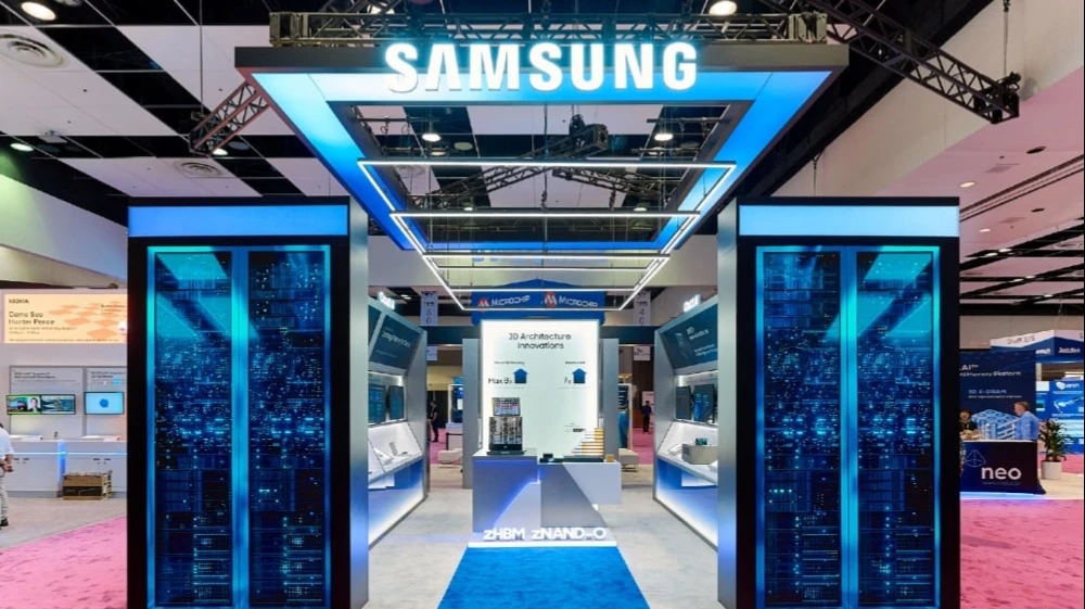
Samsung Unveils New Memory Architecture / Photo: Samsung
Samsung, the world's largest manufacturer of memory chips, has unveiled a new generation of artificial intelligence technologies. Seeking to strengthen its position amid the rapidly growing AI market, the South Korean giant is focusing on increased performance and energy efficiency to outpace its competitors—SK Hynix and Micron, according to Bloomberg.
What Samsung Showed
Samsung unveiled several new developments at its annual "Future of Memory and Storage" conference in the U.S. Their overall goal is to improve the performance and energy efficiency of artificial intelligence systems, according to Reuters.
— The most significant innovation is the zHBM architecture, which changes the way chips are arranged. Typically, High-Bandwidth Memory (HBM) is located on the board next to the processor, which results in data transfer delays. Samsung has introduced a system in which memory chips are mounted directly on top of AI accelerators, thereby minimizing the distance.
According to Samsung’s estimates, this architecture will deliver approximately an eightfold increase in performance compared to traditional systems and allow for ten times more memory. The company uses HBM5—the next-generation memory that has not yet been released—as a benchmark. In addition, the zHBM solution consumes one-third as much power, generates half the heat, and allows for flexible customization of components to meet specific customer requirements.
The company has not disclosed the dates for the widespread rollout of the vertical architecture, according to Bloomberg.
— Samsung also announced the zNAND-O architecture, designed to run real-time AI applications with minimal latency.
— In addition, a prototype of the V10 Bonding V-NAND flash memory—or BV-NAND for short—was unveiled. Its key feature is more than 400 layers stacked on top of one another. To create such a “multi-layered” chip, engineers used advanced wafer-bonding technology—essentially, the direct bonding of silicon wafers. As a result, the new drive can store 58% more data compared to the previous-generation V9 NAND. In addition, this memory offers faster data read and write speeds.
— In addition, the company presented a roadmap for the production of “smart” chips capable of partially processing data directly within the memory itself.
In the second half of the year, the company plans to ramp up production of HBM4—the most advanced generation of memory available on the market. The timeline for the transition to HBM5 is not yet known.
Why Is This Important?
Samsung unveiled its new developments amid intensifying competition in the memory market, which Bloomberg estimates to be worth nearly $1 trillion. The company is competing for customers with two other industry leaders—SK Hynix and Micron. The announcement of the new zHBM architecture reflects Samsung’s ambition to become a full-spectrum solutions provider for the AI era, Bloomberg explains.
The focus on new technologies is driven by the growing needs of the AI industry. As artificial intelligence becomes more widespread, there is an increasing need for computing power—not only to train models but also to support their day-to-day operations, such as generating responses for users. This is driving demand for various types of memory: HBM is needed for fast data exchange with AI accelerators, while NAND flash memory is required to store the large data sets needed for AI models to function.
This article was AI-translated and verified by a human editor